The Five Layers of AI Optical Interconnects
Executive Summary
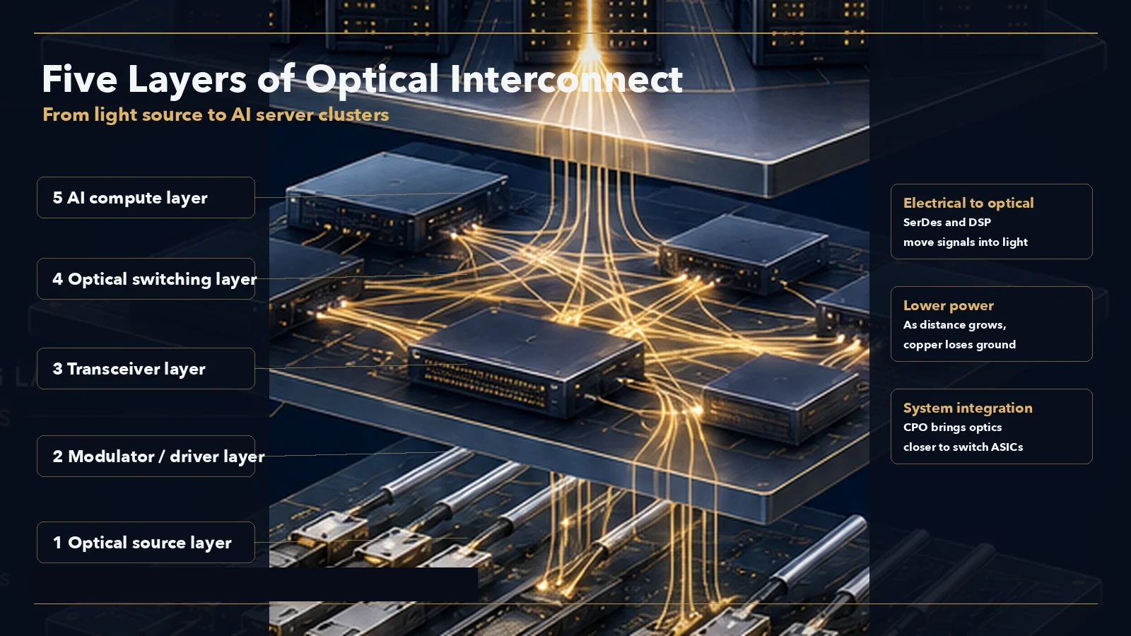
AI optical interconnects are often reduced to an optical-module story. That is too simple. The real stack has at least five layers: InP substrates, optical chips, module assembly, DSP and electrical processing, and silicon photonics / co-packaged optics.
The key question is not which stock moved the most. It is which layer is hardest to replace. Japan and the U.S. remain strong in upstream materials, optical chips, and signal-processing layers. Taiwan is building a new bottleneck in silicon-photonics foundry and co-packaged optics. China is powerful in module assembly and selected optical components, but that strength is more engineering, delivery, and cost than absolute physical scarcity.
Why “Optical Modules” Is Too Crude
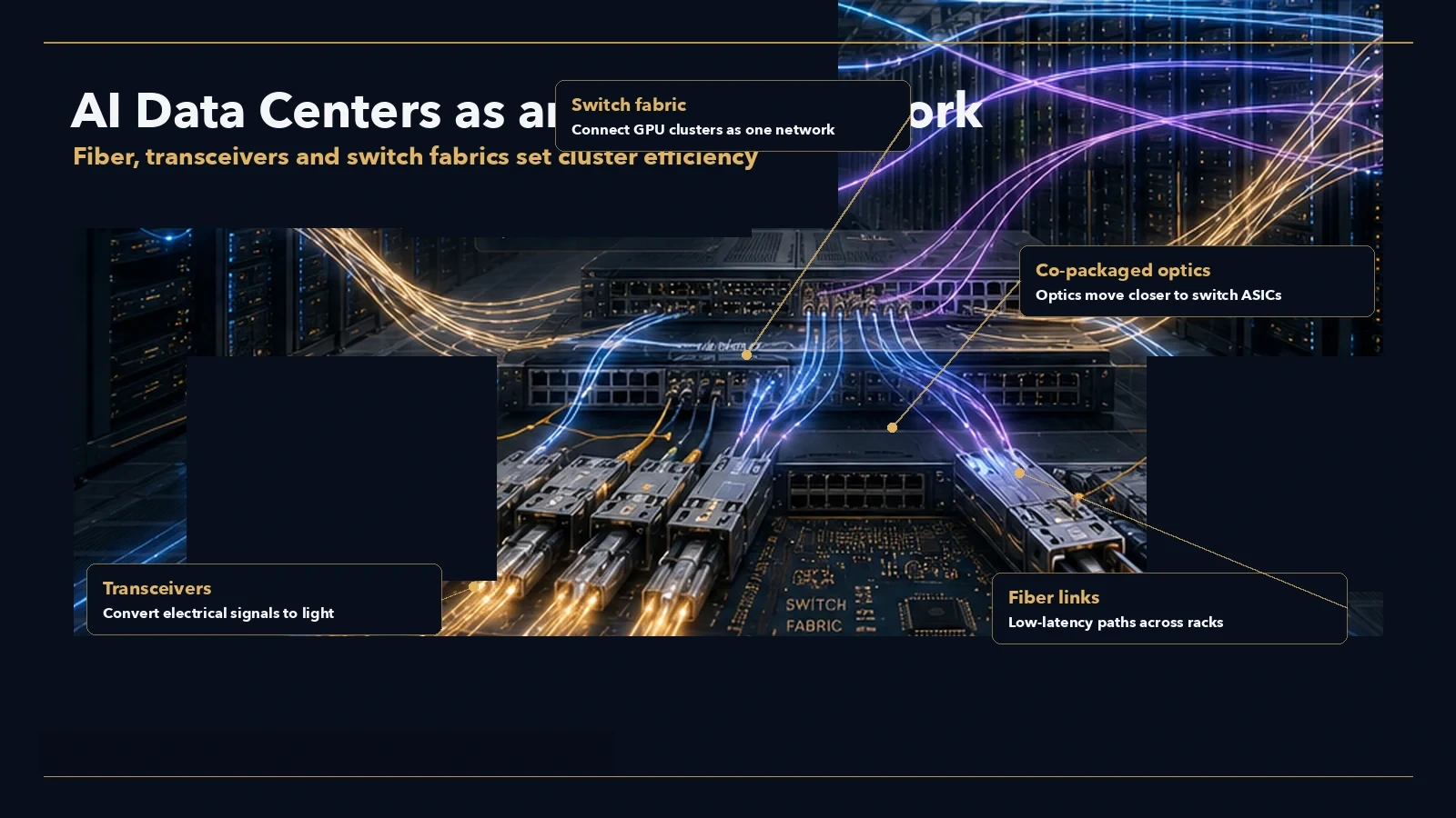
An optical module looks like one box. Inside the box sit many layers of power. The laser chip may come from a U.S. or Japanese supplier. The InP substrate may come from Japan. Some optical components may come from China. The DSP may come from a U.S. chip company. The final module may be assembled by a Chinese manufacturer and inserted into a network built around switches and accelerators.
Putting all of that under one label hides the real economics. Substrates are about materials and defects. Optical chips are about speed, modulation, and qualification. Module assembly is about scale and delivery. DSP is about electrical signal processing. Co-packaged optics are about system architecture. They all benefit from AI data-center demand. They do not all carry the same pricing power.
Layer One: InP Substrates
High-end optical communication cannot rely only on ordinary silicon. Many light-emitting devices require III-V compound semiconductors, and InP substrates form part of that base. Stable production of large, low-defect InP wafers is concentrated in a small number of suppliers.
The barrier here is materials growth, defect control, scale-up, and long customer qualification. It is less visible than final modules, but it defines the upstream capacity boundary. The counterpoint is that co-packaged and shared-laser architectures may reduce the amount of discrete laser content required per unit of bandwidth over time.
Layer Two: Optical Chips
EML, VCSEL, CW laser, and related optical chips are the heart of the link. AI data centers are moving from 800G toward 1.6T and 3.2T, which raises the bar for per-lane speed, power, and stability. If 200G/lane EML becomes the standard for high-end modules, the companies that can qualify and manufacture those devices at scale gain bargaining power.
This is where the cross-border split is sharpest. U.S. and Japanese suppliers are stronger in high-end optical chips. Chinese module companies are strong in final delivery, but still rely on external supply for parts of the high-end optical-chip layer. Chinese suppliers are moving upstream, but the hard part is not producing a sample. It is stable volume production, customer qualification, and staying close through the next specification transition.
Layer Three: Module Assembly
Chinese companies are very strong in module assembly. Innolight, Eoptolink, TFC, and peers represent engineering delivery, cost control, customer responsiveness, and manufacturing scale. This is not a layer without moat. Customer qualification, shipment history, and scale curves are real barriers.
But the barrier is different from upstream materials or optical chips. Module assembly is an engineering-system advantage. Substitution is hard because of trust and delivery efficiency, not because of one irreplaceable physics node. In a strong demand phase, the assembly layer can show high price elasticity. When customers multi-source or pricing pressure returns, that elasticity can change quickly.
Layer Four: DSP and Electrical Processing
High-speed optics are not only optical. DSPs, retimers, drivers, TIAs, and analog front-end devices handle shaping, correction, and electro-optical conversion. Broadcom, Marvell, Ciena, Semtech, MACOM, and other U.S. suppliers have deep positions here.
Co-packaged optics create tension for this layer. Pluggable modules need longer electrical paths and more signal processing. CPO moves the optical engine closer to the switch or compute die, reducing copper distance and potentially lowering some DSP requirements. For DSP suppliers, this is not a simple tailwind. It is a redistribution of the old profit pool into a new architecture.
Layer Five: Silicon Photonics and Co-Packaged Optics
Co-packaged optics are the next battleground. They bring optical engines closer to switch or compute silicon, reducing copper losses, lowering power, and increasing bandwidth density. That binds optical packaging, silicon-photonics foundry, advanced packaging, and system design into one problem.
Taiwan’s position matters here. TSMC’s silicon-photonics and advanced-packaging capabilities, Taiwan’s optical-component suppliers, and global connector and fiber-array specialists form part of the CPO ecosystem. U.S. firms define much of the switch and system architecture. Japan and Europe provide upstream support. China remains more of a follower in this layer.
The Countercase: Assembly May Be Harder Than It Looks
One mistake is to dismiss the assembly layer too quickly. Chinese module companies have not been easily replaced. They have expanded share through engineering, cost, and customer delivery. Qualification cycles, scale curves, supply-chain coordination, and delivery stability can all become competitive barriers.
The better conclusion is not that upstream is always superior and assembly is always weak. It is that barriers have different time horizons. Materials and optical chips are slower variables. Module assembly is a faster variable tied to demand and customer allocation. Co-packaged optics are the new variable. Research should keep those layers separate.
What We Do Not Know
Public disclosure is limited on optical-chip shares, customer mix, EML self-supply, and CPO volume timing. Many numbers come from industry research, brokerage estimates, or media reporting, and definitions vary. This article treats those figures as structural clues rather than precise truths.
The next variables to track are: stable production and qualification of 200G/lane EML, the move from CPO samples to volume deployments, and real progress by Chinese module companies into upstream optical components or silicon photonics.
Data and Sources
Sources are public web materials. Coverage is limited to major U.S., Chinese, Japanese, and Taiwanese optical-interconnect nodes, not a full global supply-chain scan.
This report is independent KSINQ market research and personal commentary for informational purposes only. It does not constitute investment advice. Data snapshot: June 2, 2026; rewrite date: July 2, 2026.