The World Map Inside an AI Chip
Executive Summary
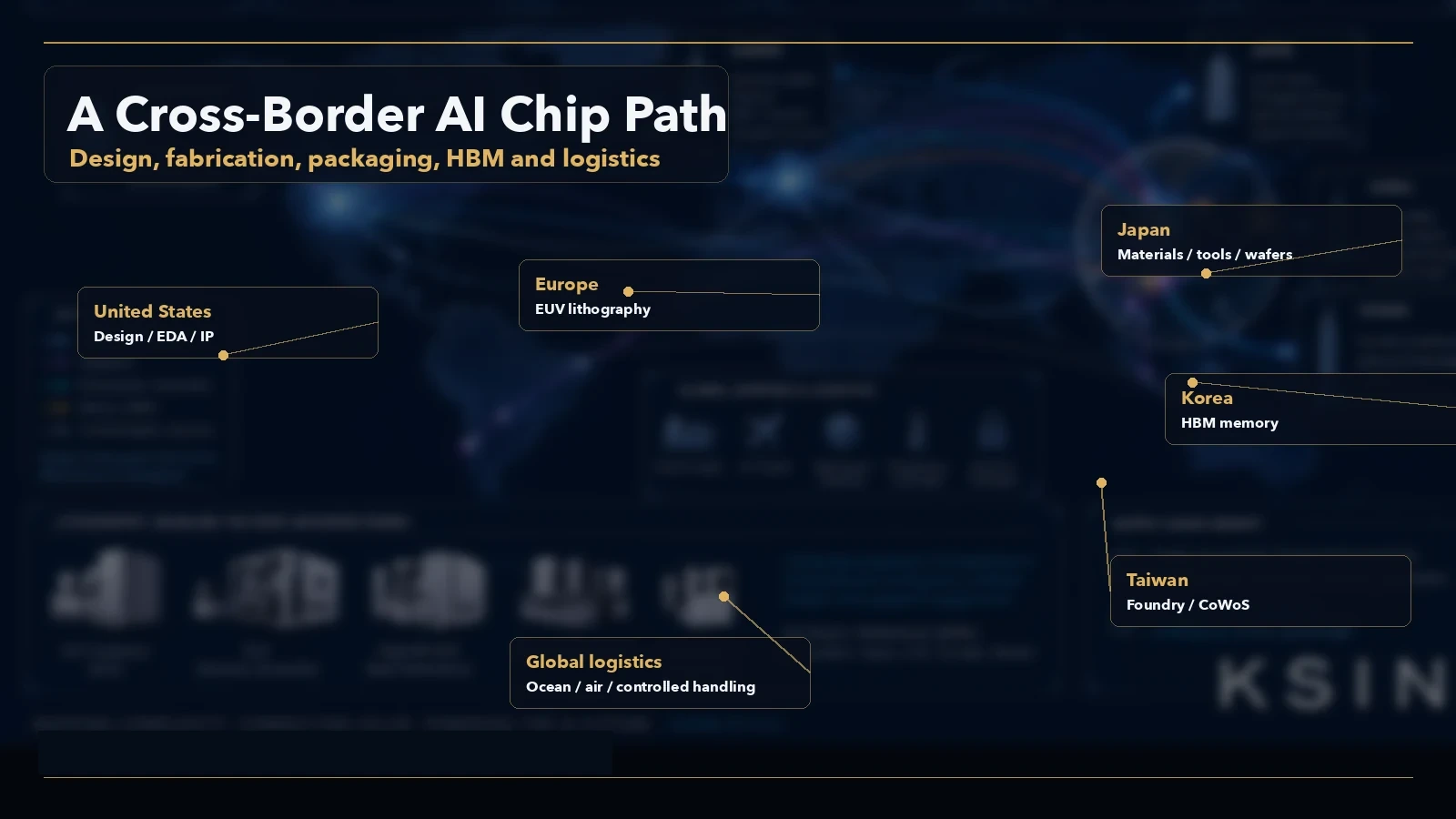
The label on a high-end accelerator may say NVIDIA, AMD, or Broadcom. The industrial system behind it is much wider: U.S. firms define architecture and EDA, ASML supplies EUV lithography, Taiwan manufactures and packages, Korea supplies HBM, Japan provides critical tools and materials, and the final server chain turns chips into deployable systems.
This piece is not a ranking of individual stocks. It asks where the industrial power sits inside the AI chip chain. The short answer: benchmark scores move the story; bottlenecks move the supply curve.
Why Design and Manufacturing Split Apart
The modern semiconductor chain rests on the separation between fabless design and foundry manufacturing. Design firms own architecture, software, verification, and customer roadmaps. Foundries concentrate the capital-intensive manufacturing layer.
That division exists because advanced fabs are too expensive to serve only one internal product line. The fixed cost has to be spread across many customers, many chip designs, and many years of utilization. The same logic explains why a fabless company can capture very high system value while a foundry without the consumer-facing brand can still control the delivery schedule.
The visible brand is not always where the constraint sits. Power in this chain comes from scarcity, certification, yield learning, and the difficulty of customer substitution.
Advanced Packaging Became a System Layer
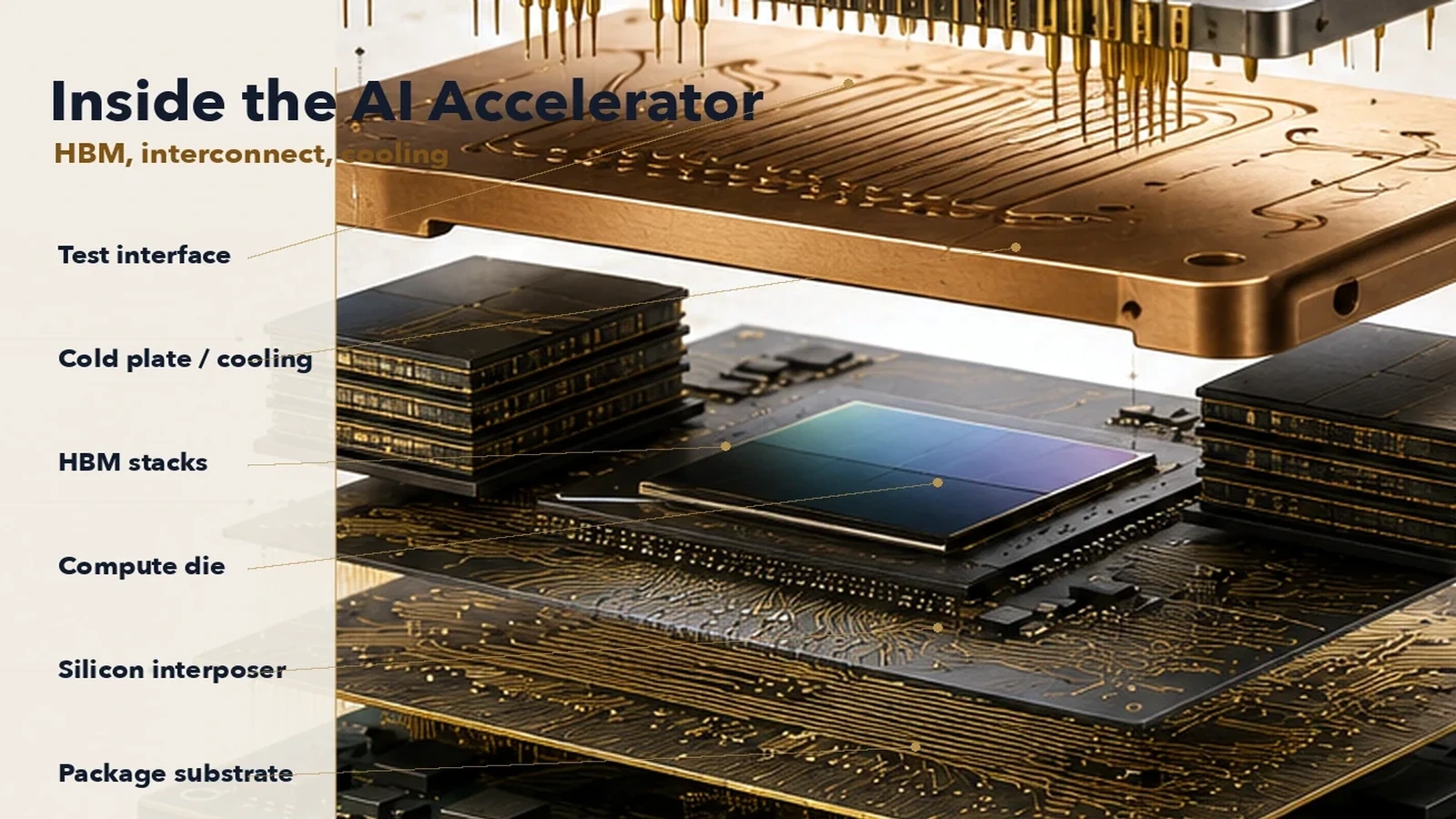
AI accelerators have pushed packaging from a back-end wrapper into a system architecture layer. Very large monolithic dies run into reticle limits, yield problems, and cost. The industry response is to assemble GPU or ASIC dies, HBM stacks, I/O dies, and interposers into one package-level system.
CoWoS, SoIC, EMIB, Foveros, and hybrid bonding may sound like packaging jargon. In AI systems, they decide whether theoretical compute can be shipped as usable hardware. HBM makes the point clearer. It is not simply a better DRAM chip. It is a stacked memory system placed close enough to the accelerator to feed it with bandwidth.
That is why AI chip supply should not be read only through design roadmaps. The more important questions are whether CoWoS capacity is available, whether HBM stacking yield is stable, whether packaging tools and materials can keep up, and whether customer platform qualification happens on time.
Node Names Are Not the Whole Answer
Process node names still matter, but they are no longer sufficient. N2, 18A, A16, and other labels need to be decomposed into transistor architecture, backside power, EUV or High-NA tool access, yield learning, and customer adoption.
GAA nanosheet structures address electrostatic control at smaller geometries. Backside power delivery reduces front-side routing congestion. Intel’s 18A with RibbonFET and PowerVia, TSMC’s N2/A16 path, and Samsung’s GAA roadmap should be judged by stable customer delivery rather than marketing numbers alone.
This is also the real test for Intel’s foundry ambitions. A roadmap can show a narrowing technology gap. A foundry business still has to earn trust on capacity, yield, packaging, IP, and ecosystem risk.
The Cross-Border Path of One GPU
The process map is highly international.
The first layer is design and software, led by U.S. firms. NVIDIA, AMD, Broadcom, and others define architectures; Synopsys and Cadence convert designs into manufacturable layouts.
The second layer is lithography. ASML’s EUV systems remain unavoidable for the most advanced nodes. EUV itself depends on a deeper European optics, laser, and component chain.
The third layer is foundry and packaging. TSMC is the central node for advanced process and CoWoS-style packaging. In many AI chips, the constraint is not whether the design exists; it is whether the package can be produced at scale.
The fourth layer is memory. SK hynix, Samsung, and Micron define the HBM supply curve. Their qualification progress and generation transitions can alter accelerator delivery schedules.
The fifth layer is Japanese tools and materials. Wafers, photoresists, coaters, developers, inspection tools, cleaning systems, and specialty materials are less visible than final brands, but they keep the manufacturing system running.
The sixth layer is test, assembly, and server integration. ASE, Amkor, Foxconn, Quanta, Wistron, and peers connect chip packages to boards, systems, racks, and customers. They may not always own the hardest single bottleneck, but they shape delivery speed.
The Countercase: Can Bottlenecks Be Copied?
The opposing case deserves respect. Any high-margin bottleneck attracts capex, subsidies, and customer multi-sourcing. CoWoS tightness invites expansion. HBM profitability invites competition among the three suppliers. Geopolitical pressure on EDA and lithography encourages substitution projects.
But being challenged is not the same as being replaceable. Semiconductor bottlenecks are cumulative systems of process knowledge, qualification history, yield curves, maintenance capability, and supply-chain coordination. A lab demonstration does not equal industrial substitution.
A cleaner framework separates bottlenecks into three groups. Absolute bottlenecks include EUV lithography and certain EDA layers. Cyclical or phase bottlenecks include CoWoS, HBM, and hybrid bonding capacity. Engineering-scale bottlenecks include server integration and parts of the packaging chain. All three matter. They do not have the same durability.
What We Do Not Know
This article is adapted from prior research materials and public sources. It is not a full semiconductor equity screen and does not update every supplier’s latest financials. Some capacity, share, and customer-allocation numbers come from industry research or media estimates, and their definitions can change by quarter.
The next questions to track are straightforward: whether advanced packaging remains the shipment ceiling, whether HBM multi-sourcing changes margin distribution, and whether new process nodes are validated by real customer ramps. If all three improve, the tight constraint in AI chips moves downstream. If one fails, benchmark narratives will still meet physical delivery limits.
Data and Sources
Sources are public web materials. Coverage is limited to major AI chip supply-chain nodes, not the whole semiconductor market.
This report is independent KSINQ market research and personal commentary for informational purposes only. It does not constitute investment advice. Data snapshot: June 1, 2026; rewrite date: July 2, 2026.